- 您现在的位置:买卖IC网 > Sheet目录2003 > LTC1337CNW#PBF (Linear Technology)IC 3DVR/5RCVR 5V RS232 28-DIP
4
LTC1337
1337fa
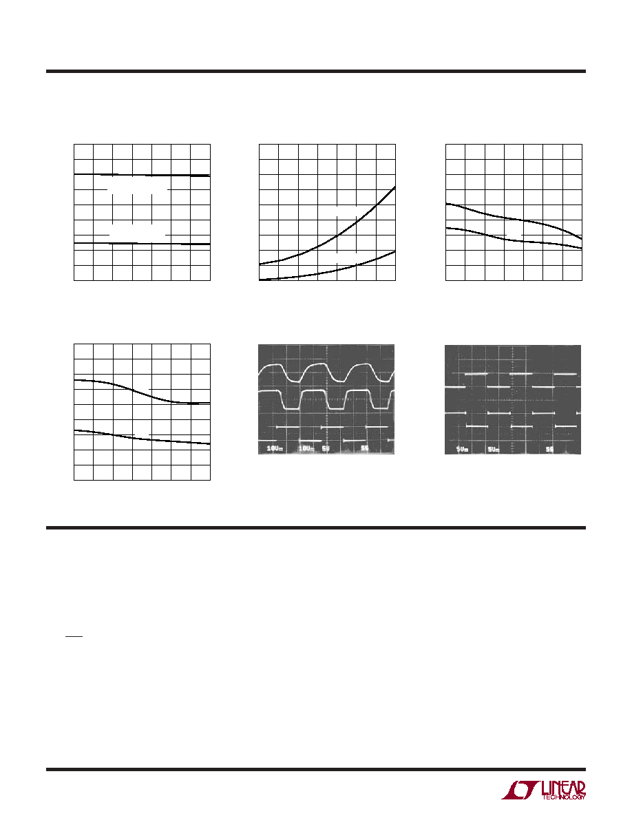
TYPICAL PERFOR A CE CHARACTERISTICS
UW
VCC Supply Current
TEMPERATURE (°C)
0
LEAKAGE
CURRENT
(
A)
60
45
40
35
30
25
20
15
10
5
0
1337 G05
20
70
10
30
40
50
VOUT = –20V
VOUT = 20V
TEMPERATURE (°C)
0
SUPPLY
CURRENT
(mA)
60
20
16
14
12
10
8
6
4
2
0
1337 G04
20
70
10
30
40
50
3 DRIVERS LOADED
RL = 3k
1 DRIVER LOADED
RL = 3k
Driver Short-Circuit Current
Driver Leakage in Shutdown
Receiver Short-Circuit Current
Driver Output Waveforms
INPUT
DRIVER
OUTPUT
RL = 3k
DRIVER
OUTPUT
RL = 3k
CL = 2500pF
Receiver Output Waveforms
RX
OUTPUT
CL = 50pF
INPUT
TEMPERATURE (°C)
0
SHORT-CIRCUIT
CURRENT
(mA)
60
20
18
16
14
12
10
8
6
4
2
1337 G06
20
70
10
30
40
50
ISC
+
ISC
–
TEMPERATURE (°C)
0
SHORT-CIRCUIT
CURRENT
(mA)
60
55
50
45
40
35
30
25
20
15
10
1337 G07
20
70
10
30
40
50
ISC
+
ISC
–
UU
U
PI FU CTIO S
VCC: 5V Input Supply Pin. Supply current less than 1A in
the Shutdown mode. This pin should be decoupled with a
0.1F ceramic capacitor.
GND: Ground Pin.
ON/OFF: TTL/CMOS Compatible Shutdown Pin. A logic
low puts the device in the Shutdown mode which reduces
input supply current to less than 1A and places all drivers
and receivers in high impedance state. This pin cannot
float.
V+: Positive Supply Output (RS232 Drivers). V+ 2VCC –
1V. This pin requires an external capacitor C = 0.1F for
charge storage. The capacitor may be tied to ground or 5V.
With multiple devices, the V + and V – pins may be paral-
leled into common capacitors. For large numbers of
devices, increasing the size of the shared common storage
capacitors is recommended to reduce ripple.
V–: Negative Supply Output (RS232 Drivers). V– (2VCC
–1.5V). This pin requires an external capacitor C = 0.1F
for charge storage.
C1+, C1–, C2+, C2–: Commutating Capacitor Inputs. These
pins require two external capacitors C = 0.1F. One from
C1+ to C1–, and another from C2+ to C2–. To maintain
charge pump efficiency, the capacitor’s effective series
resistance should be less than 50.
发布紧急采购,3分钟左右您将得到回复。
相关PDF资料
LTC1382IN#PBF
IC TXRX 5V RS232 W/SHTDWN 18-DIP
LTC1383IS#TRPBF
IC TXRX 5V RS232 LOW PWR 16-SOIC
LTC1384IG#TRPBF
IC TXRX 5V RS232 LOW PWR 20-SSOP
LTC1385IN#PBF
IC TXRX 3.3V EIA/TIA-562 18-DIP
LTC1386IS#TRPBF
IC TXRX 3.3V EIA/TIA-562 16-SOIC
LTC1387IG#TRPBF
IC TXRX RS232/RS485 5VSNGL20SSOP
LTC1400IS8
IC A/D CONV 12BIT W/SHTDN 8-SOIC
LTC1401IS8#TRPBF
IC A/D CONV 12BIT W/SHTDN 8-SOIC
相关代理商/技术参数
LTC1337CSW
功能描述:IC 3DVR/5RCVR 5V RS232 28-SOIC RoHS:否 类别:集成电路 (IC) >> 接口 - 驱动器,接收器,收发器 系列:- 标准包装:27 系列:- 类型:收发器 驱动器/接收器数:3/3 规程:RS232,RS485 电源电压:4.75 V ~ 5.25 V 安装类型:表面贴装 封装/外壳:28-SOIC(0.295",7.50mm 宽) 供应商设备封装:28-SOIC 包装:管件
LTC1337CSW#PBF
功能描述:IC 3DVR/5RCVR 5V RS232 28-SOIC RoHS:是 类别:集成电路 (IC) >> 接口 - 驱动器,接收器,收发器 系列:- 标准包装:27 系列:- 类型:收发器 驱动器/接收器数:3/3 规程:RS232,RS485 电源电压:4.75 V ~ 5.25 V 安装类型:表面贴装 封装/外壳:28-SOIC(0.295",7.50mm 宽) 供应商设备封装:28-SOIC 包装:管件
LTC1337CSW#TR
功能描述:IC TXRX RS232 5V LOW PWR 28SOIC RoHS:否 类别:集成电路 (IC) >> 接口 - 驱动器,接收器,收发器 系列:- 标准包装:27 系列:- 类型:收发器 驱动器/接收器数:3/3 规程:RS232,RS485 电源电压:4.75 V ~ 5.25 V 安装类型:表面贴装 封装/外壳:28-SOIC(0.295",7.50mm 宽) 供应商设备封装:28-SOIC 包装:管件
LTC1337CSW#TRPBF
功能描述:IC 3DVR/5RCVR 5V RS232 28-SOIC RoHS:是 类别:集成电路 (IC) >> 接口 - 驱动器,接收器,收发器 系列:- 标准包装:27 系列:- 类型:收发器 驱动器/接收器数:3/3 规程:RS232,RS485 电源电压:4.75 V ~ 5.25 V 安装类型:表面贴装 封装/外壳:28-SOIC(0.295",7.50mm 宽) 供应商设备封装:28-SOIC 包装:管件
LTC1338CG
功能描述:IC 5DVR/3RCVR 5V RS232 28-SSOP RoHS:否 类别:集成电路 (IC) >> 接口 - 驱动器,接收器,收发器 系列:- 标准包装:250 系列:- 类型:收发器 驱动器/接收器数:2/2 规程:RS232 电源电压:3 V ~ 5.5 V 安装类型:表面贴装 封装/外壳:16-TSSOP(0.173",4.40mm 宽) 供应商设备封装:16-TSSOP 包装:带卷 (TR)
LTC1338CG#PBF
功能描述:IC 5DVR/3RCVR 5V RS232 28-SSOP RoHS:是 类别:集成电路 (IC) >> 接口 - 驱动器,接收器,收发器 系列:- 标准包装:1 系列:- 类型:线路收发器 驱动器/接收器数:5/3 规程:RS232 电源电压:3 V ~ 5.5 V 安装类型:表面贴装 封装/外壳:28-SOIC(0.295",7.50mm 宽) 供应商设备封装:28-SOIC 包装:Digi-Reel® 产品目录页面:918 (CN2011-ZH PDF) 其它名称:296-25096-6
LTC1338CG#PBF
制造商:Linear Technology 功能描述:RS232 Driver IC
LTC1338CG#TR
功能描述:IC TXRX RS232 5V LOW PWR 28SSOP RoHS:否 类别:集成电路 (IC) >> 接口 - 驱动器,接收器,收发器 系列:- 标准包装:27 系列:- 类型:收发器 驱动器/接收器数:3/3 规程:RS232,RS485 电源电压:4.75 V ~ 5.25 V 安装类型:表面贴装 封装/外壳:28-SOIC(0.295",7.50mm 宽) 供应商设备封装:28-SOIC 包装:管件